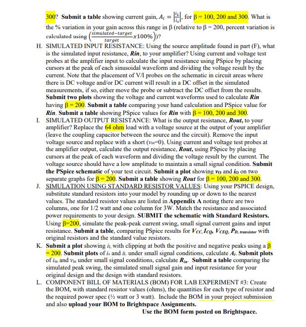
300? Submit a table showing current gain, A = for B = 100, 200 and 300. What is
the % variation in your gain across this range in ß (relative to B= 200, percent variation is
calculated using
(simulated-target x100%))?
target
H. SIMULATED INPUT RESISTANCE: Using the source amplitude found in part (F), what
is the simulated input resistance, Rin, to your amplifier? Using current and voltage test
probes at the amplifier input to calculate the input resistance using PSpice by placing
cursors at the peak of each sinusoidal waveform and dividing the voltage result by the
current. Note that the placement of V/I probes on the schematic in circuit areas where
there is DC voltage and/or DC current will result in a DC offset in the simulated
measurements, if so, either move the probe or subtract the DC offset from the results.
Submit two plots showing the voltage and current waveforms used to calculate Rin
having B= 200. Submit a table comparing your hand calculation and PSpice value for
Rin. Submit a table showing PSpice values for Rin with B = 100, 200 and 300.
I. SIMULATED OUTPUT RESISTANCE: What is the output resistance, Rout, to your
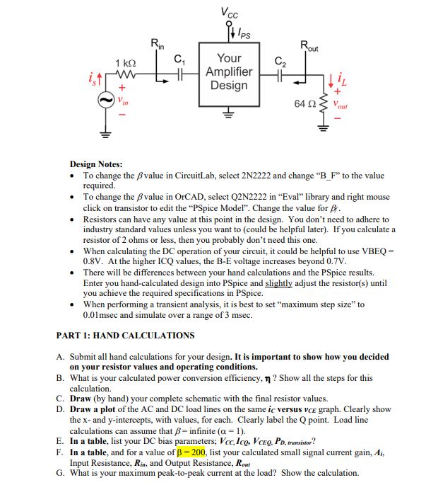
amplifier? Replace the 64 ohm load with a voltage source at the output of your amplifier
(leave the coupling capacitor between the source and the circuit). Remove the input
voltage source and replace with a short (V-0). Using current and voltage test probes at
the amplifier output, calculate the output resistance, Rout, using PSpice by placing
cursors at the peak of each waveform and dividing the voltage result by the current. The
voltage source should have a low amplitude to maintain a small signal condition. Submit
the PSpice schematic of your test circuit. Submit a plot showing vo and io on two
separate graphs for Bß = 200. Submit a table showing Rout for B = 100, 200 and 300.
J. SIMULATION USING STANDARD RESISTOR VALUES: Using your PSPICE design,
substitute standard resistors into your model by rounding up or down to the nearest
values. The standard resistor values are listed in Appendix A noting there are two
columns, one for 1/2 watt and one column for 3W. Match the resistance and associated
power requirements to your design. SUBMIT the schematic with Standard Resistors.
Using B=200, simulate the peak-peak current swing, small signal current gains and input
resistance. Submit a table, comparing PSpice results for Vcc, Ico, VCEQ, PD. transistor with
original resistors and the standard value resistors.
K. Submit a plot showing it with clipping at both the positive and negative peaks using a B
= 200. Submit plots of is and it under small signal conditions, calculate A₁. Submit plots
of fin and Vin under small signal conditions, calculate Rin- Submit a table comparing the
simulated peak swing, the simulated small signal gain and input resistance for your
original design and the design with standard resistors.
L. COMPONENT BILL OF MATERIALS (BOM) FOR LAB EXPERIMENT #3: Create
the BOM, with standard resistor values (ohms), the quantities for each type of resistor and
the required power spec (½ watt or 3 watt). Include the BOM in your project submission
and also upload your BOM to Brightspace Assignments.
Use the BOM form posted on Brightspace./nPART 2: PSPICE SIMULATIONS:
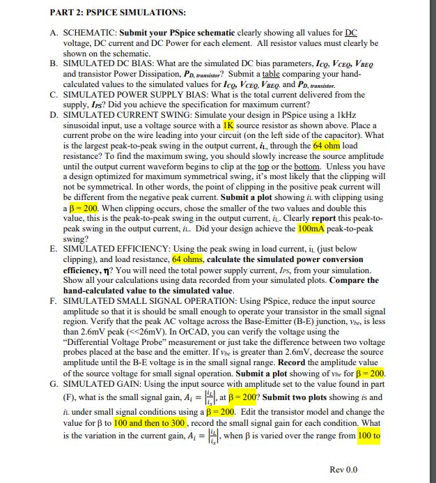
A. SCHEMATIC: Submit your PSpice schematic clearly showing all values for DC
voltage, DC current and DC Power for each element. All resistor values must clearly be
shown on the schematic.
B. SIMULATED DC BIAS: What are the simulated DC bias parameters, Ico, VCEO, VBEQ
and transistor Power Dissipation, PD, transistor? Submit a table comparing your hand-
calculated values to the simulated values for Ico, VCEO, VREQ, and PD, transistor.
C. SIMULATED POWER SUPPLY BIAS: What is the total current delivered from the
supply, Ips? Did you achieve the specification for maximum current?
D. SIMULATED CURRENT SWING: Simulate your design in PSpice using a 1kHz
sinusoidal input, use a voltage source with a 1K source resistor as shown above. Place a
current probe on the wire leading into your circuit (on the left side of the capacitor). What
is the largest peak-to-peak swing in the output current, it, through the 64 ohm load
resistance? To find the maximum swing, you should slowly increase the source amplitude
until the output current waveform begins to clip at the top or the bottom. Unless you have
a design optimized for maximum symmetrical swing, it's most likely that the clipping will
not be symmetrical. In other words, the point of clipping in the positive peak current will
be different from the negative peak current. Submit a plot showing it with clipping using
a ß = 200. When clipping occurs, chose the smaller of the two values and double this
value, this is the peak-to-peak swing in the output current, i. Clearly report this peak-to-
peak swing in the output current, iL. Did your design achieve the 100mA peak-to-peak
swing?
E. SIMULATED EFFICIENCY: Using the peak swing in load current, it (just below
clipping), and load resistance, 64 ohms, calculate the simulated power conversion
efficiency, n? You will need the total power supply current, Ips, from your simulation.
Show all your calculations using data recorded from your simulated plots. Compare the
hand-calculated value to the simulated value.
F. SIMULATED SMALL SIGNAL OPERATION: Using PSpice, reduce the input source
amplitude so that it is should be small enough to operate your transistor in the small signal
region. Verify that the peak AC voltage across the Base-Emitter (B-E) junction, Vie, is less
than 2.6mV peak (<<26mV). In OrCAD, you can verify the voltage using the
"Differential Voltage Probe" measurement or just take the difference between two voltage
probes placed at the base and the emitter. If he is greater than 2.6mV, decrease the source
amplitude until the B-E voltage is in the small signal range. Record the amplitude value
of the source voltage for small signal operation. Submit a plot showing of the for B= 200.
G. SIMULATED GAIN: Using the input source with amplitude set to the value found in part
(F), what is the small signal gain, A = at B= 200? Submit two plots showing is and
iL under small signal conditions using a ß = 200. Edit the transistor model and change the
value for 3 to 100 and then to 300, record the small signal gain for each condition. What
is the variation in the current gain, A₁ = when ẞ is varied over the range from 100 to
Rev 0.0/nIm
•
•
1 ΚΩ
Design Notes:
•
in
Rin
[
C₁
Vcc
Ips
Your
Amplifier
Design
1
64 02 V
Rout
C₂
out
value in CircuitLab, select 2N2222 and change "B_F" to the value
To change the
required.
To change the
value in OrCAD, select Q2N2222 in "Eval" library and right mouse
click on transistor to edit the "PSpice Model". Change the value for fr.
Resistors can have any value at this point in the design. You don't need to adhere to
industry standard values unless you want to (could be helpful later). If you calculate a
resistor of 2 ohms or less, then you probably don't need this one.
• When calculating the DC operation of your circuit, it could be helpful to use VBEQ =
0.8V. At the higher ICQ values, the B-E voltage increases beyond 0.7V.
•
There will be differences between your hand calculations and the PSpice results.
Enter you hand-calculated design into PSpice and slightly adjust the resistor(s) until
you achieve the required specifications in PSpice.
When performing a transient analysis, it is best to set "maximum step size" to
0.01 msec and simulate over a range of 3 msec.
PART 1: HAND CALCULATIONS
A. Submit all hand calculations for your design. It is important to show how you decided
on your resistor values and operating conditions.
B. What is your calculated power conversion efficiency, ? Show all the steps for this
calculation.
C. Draw (by hand) your complete schematic with the final resistor values.
D. Draw a plot of the AC and DC load lines on the same ic versus VCE graph. Clearly show
the x- and y-intercepts, with values, for each. Clearly label the Q point. Load line
calculations can assume that = infinite (a = 1).
E. In a table, list your DC bias parameters; Vcc, Ico, VCEQ, PD, transistor?
F. In a table, and for a value of ß = 200, list your calculated small signal current gain, Ai,
Input Resistance, Rin, and Output Resistance, Rout
G. What is your maximum peak-to-peak current at the load? Show the calculation.