Question 2 (60 marks)
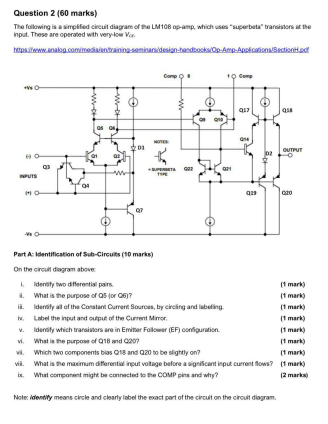
The following is a simplified circuit diagram of the LM108 op-amp, which uses "superbata" transistors at the
input. These are operated with very low Vo
https://www.analog.com/media/entraining seminars/design-handbooks/Op-Amp-Applications/Section.pdf
H
INPUTS
MO
V
a
1.
.
ii.
Q3
as 0
01
201
Q7
Part A: Identification of Sub-Circuits (10 marks)
On the circuit diagram abover
Comp
wWw
SUPE022
010
10 Comp
configuration.
Q17
019
Qu
Identify two differential pairs
What is the purpose of Q5 (or Q6)?
Identify all of the Constant Current Sources, by circling and labelling
Label the input and output of the Current Mirror.
Identify which transistors are in Emitter Follower (EF)
vi.
What is the purpose of Q18 and 207
vii. Which two components bias Q18 and 920 to be slightly on?
(1 mark)
vii. What is the maximum differential input voltage before a significant input current flows? (1 mark)
ix. What component might be connected to the COMP pins and why?
(2 marks)
Note: Identify means circle and clearly label the exact part of the circuit on the circuit diagram.
OUTPUT
0:20
(1 mark)
(1 mark)
(1 mark)
(1 mark)
(1 mark)/nPart B: Hand Analyses (20 marks)
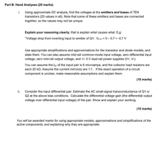
Using approximate DC analysis, find the voltages at the emitters and bases of TEN
transistors (20 values in all). Note that some of these emitters and bases are connected
together, so the values may not be unique
Explain your reasoning clearly, that is explain what causes what. Eg:
"Voltage drop from inverting input to emitter of Q1: V-0-07-07 V
Use appropriate simplifications and approximations for the transistor and diode models, and
state them. You can also assume mid-rail common-mode input voltage, zero differential input
voltage, zero mid-raill output voltage, and +-5V dual-rail power supplies (V+, V.).
You can assume the of the input pair is 6 microamps, and the collector load resistors are
each 20 k. Assume the current mirror(s) are 1:1. If the exact operation of a circult
component is unclear, make reasonable assumptions and explain them
(10 marks)
i Consider the input differential pair. Estimate the AC small-signal transconductance of Q1 or
Q2 at the above bias conditions Calculate the differential voltage gain (the differential output
voltage over differential input voltage) of the pair. Show and explain your working.
(10 marks)
You will be awarded marks for using appropriate models, approximations and simplifications of the
active components, and explaining why they are appropriate/nPart C: Simulations (30 Marks)
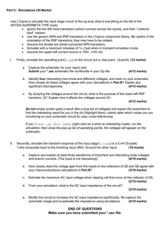
Use LTspice to simulate the input stage circuit of the op-amp (that is everything to the left of the
NOTES-SUPERBETA TYPE inst
• Ignore the two left-most transistors (which connect across the inputs), and their "collector
• Use the generic NPN and PNP transistors in the LTspice component library. Be careful of the
orientation of the PNP transistors; they may have to be rotated.
• Assume the diodes are diode-connected NPN transistors.
• Simulate with a maximum timestep of tu (us) when in transient simulation mode
• Assume the upper-left current source is 100n (100 nA)
i. Firstly, simulate the operating point (op) on the circuit (aka blas point, Q-point) (12 marks)
a
Capture the schematic for your report and
Submit your "ase schematic file via Moodle in your Zip file.
(4/12 marks)
b. Identify four interesting (non-trivial and different) voltages, and mark on your schematic.
How closely do these voltages agree with your calculations in Part B7 Explain any
significant discrepancies.
(4/12 marks)
By studying the voltages around the circuit, what is the purpose of the lower-left PNP
transistor, Q7. Explain how it affects the voltages around Q1.
(4/12 marks)
Do not simply screen grab a result like a long list of voltages) and expect the examiners to
find the interesting result for you in the ist (highlight them clearly label which nodes you are
monitoring on your schematic circult for easy cross-referencing
If you Place op Data Label (right click on a wine) on interesting nodes, run the
simulation, then close the pop-up kat of operating points, the voltages will appear on the
schematic
1. Secondly, simulate the transient response of the input stage (.tran) to a 5 mV (0-peak)
1-kHz sinusoidal input to the Inverting input (INV). Ground the other inpur (18 marks)
a
Capture and explain at least three waveforms of important and interesting node voltages
and branch currents. (The input is not interesting).
(6/18 marks)
b. How closely does the voltage gain from the inputs to the collectors of Q5 and Q6 agree with
your transconductance calculations in Part B?
(3/18 marks)
c. Estimate the maximum AC input voltage when clipping will first occur at the collector of Q5.
(2/18 marks)
d. From your simulation, what is the AC input impedance of the circuit?
(3/18 marks)
e Modify the circuit to increase the AC input impedance significantly. Re-capture the
schematic image and re-estimate the impedance using simulations (4/18 marks)
END OF QUESTIONS
Make sure you have submitted your "ase file.